PCB Design

Expert Printed Circuit Board Design services provided by our affiliate partner, Synergy Circuits
Synergy Circuits PCB Design Company
Finished Printed Circuit Board
Printed Circuit Board Design

PCB Design

Start to Finish PCB Development

Printed Circuit Board (PCB) Design is offered by our affiliate partner Synergy Circuits. Locally headquartered in San Jose, California, Synergy Circuits is an ISO certified and ITAR registered company.

Synergy Circuits specializes in end-to-end PCB development as well as PCB cost optimization. Synergy’s strong knowledge of Gorilla Circuits manufacturing capabilities (DFM) and cost drivers help to evaluate the PCB design for cost optimization. Synergy Circuits boasts over 20 years of design experience, ensuring a knowledgeable PCB Design experience!
Printed Circuit Board Design brought to you by affiliate partner,
Synergy Circuits

PCB Design Services

PCB Engineering
  • Circuit Design
  • Simulations/Modeling
  • Validation
PCB Design/ Layout
  • Schematic Capture
  • PCB Layout Design
  • DFM/DFA analysis
PCB Optimization
  • Optimize current PCB designs for cost
Validation
  • ICT testing/Flying Probe Continuity Testing
  • VNA
Product Types
  • ATE Test boards (Load board and Probe card, Wafer test & Burn in Boards)
  • Medical Products
  • Industrial PCB products
  • Commercial/Mobile products
  • Telecom Infrastructure
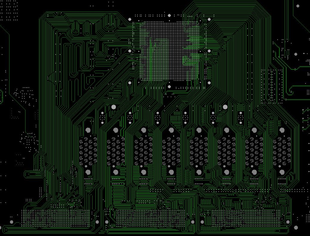
Delay Matched Routing PCB Design Example
PCB Design by affiliate partner, Synergy Circuits

Customer Service

24/7 Design Cycle

We support our customers for quick turn around times with a day shift in US and two shifts in India.

Video Chat with us via GoToMeeting

Join a video chat with our Design team for layout and schematic review.

On-site Support

Experience Application engineers available for on-site customer support, if required.

Start to Finish

Our design team is available for support in any stage of the design!
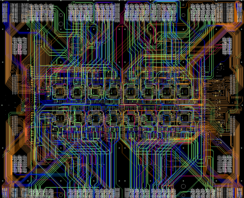
 
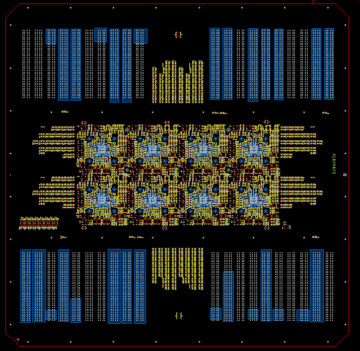
ATE Board PCB Design Example
Brought to you by affiliate partner, Synergy Circuits

PCB Layout Services

Library Management
  • Custom component footprints and verification created
  • Separate library database for all our clients established
  • 3D models generated for parts, which are also incorporated into the corresponding footprints
24-hour Routing Service Model
  • We partition the design among multiple designers to achieve efficient output, we run 24 hours: a day shift in the United States and two “overnight” shifts in India
  • Customer time zone assessed and files reviewed for AM file delivery, giving seamless design continuation for the customer
  • Once the customer is done for the day, the file is returned to us for design progress to achieve a 24-hour design output cycle
Manufacturing Package and DFM/DFA Analysis
  • All the manufacturing files are gathered from the customer CAD data
  • Complete DFM/DFA services for small batch prototypes are provided, as well as comprehensive DFM/DFA analysis for mass production
 

Let’s Build Something Incredible!

Synergy Circuits Design Tools

Design Tools

  • Cadence Allegro 17.4, 17.2, 16.6
  • Mentor Graphics PADS
  • Altium Designer
  • Schematic Capture: Orcad, Concept HDL and PADS Logic
  • AutoCAD and Valor Genesis 10.1
  • SI/PI simulations
PCB Design by affiliate partner, Synergy Circuits

Design Capabilities

  • Analog/Digital, RF/Microwave, Mixed signal/High speed designs
  • HDI Design for fine pitch BGA circuitry
  • PCB Designs up to 64 layers
  • Fine pitch BGA’s (multi-site .3mm and .4mm pitch BGA) ATE boards
  • High Speed Design 106Gbps
  • Signal integrity/cross talk analysis.
  • Layer stack up optimization
  • S-parameter measurements and channel optimization.
  • 3D/2.5D model extraction and electrical simulations
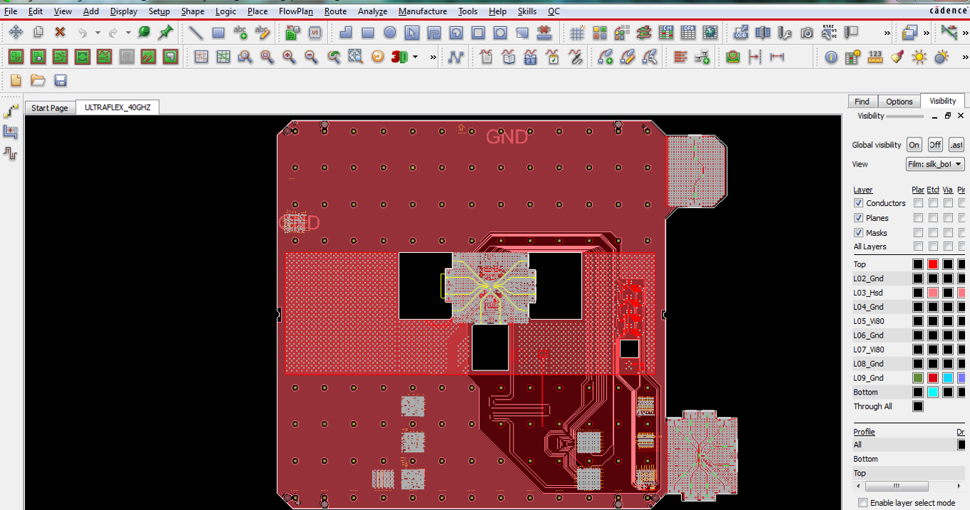
RF Signal PCB Design Example
PCB Design by affiliate partner, Synergy Circuits

RF and High Speed capabilities


Experience With:

  • Various engagements in 5G network PCB development. Test boards for BGAs designed for 5G networks. RF products related to broadcasting for 5G network requirements. Characterization PCBs for bench testing environments for 5G Applications.
  • Designing test boards for leading ATE test system Vendor’s Tester Platforms.
  • PCB Designs requiring leading interface technologies such as USB 2.0, USB 3.0, HDMI, UART, I2C, PCI, PCIe, SATA, SAS, DDR4, Ethernet PHY Interface/Serdes, and more.
  • Selecting optimum PCB materials when required including high frequency laminates (Rogers/Tachyon), high temp requirements (Arlon85n), and RF requirements (Rogers/MW2000/Tachyon100G, MT40).
  • Stack up optimization for high layer count PCBs (60 layers) and experience in handling Multiple Impedance control (50/90/100 ohm) on the same board.
  • Design of ELIC boards (Every Layer Interconnect/HDI laser/filled stacked-vias) for Smartphone or other Mobile PCB applications.

PCB Design

Synergy Circuits has a direct line of communication with our Fab Process Engineers who have the best and latest knowledge of our facilities DFM rules. Design function plays a key role in making the most challenging technologies manufacturable. We strive to streamline the design-to-manufacturing cycle with the focus on internal communication.

Lead Time

Our available 24/6 operations for Fabrication and Assembly supplements our design cycles to support critical lead time requirements.

Cost

Eliminate markups on Design, Fab, Parts, Assembly & Test. We do not broker.